


Several hundred process steps are needed for semiconductor device (memory, CPU etc.) manufacturing.
The CMP is a newly necessary process in each key process step, and it becomes more important in advanced processes that are trending toward higher density in a vertical direction.
Furthermore, CMP process have been applied for wafer thinning process (backside polishing) after grinding. This means CMP is now expanding into the packaging process area as well.
Circuit design
Silicon wafer
Pattern design
Film deposition
Photo mask making
Patterning
Photoresist coating
Ashing / Cleaning
Exposure
Development / Etching
Shallow Trench Isolation (STI)
Gate process
Contact process
Interconnect process

Post-process
Complete
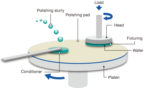
CMP process
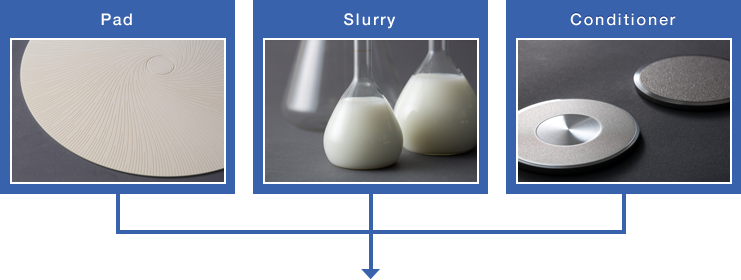
At NITTA DuPont, we have the three Imperial Regalia for the CMP process; “pads”, “slurries” and “conditioners”. This combination offering can deliver a total solution that can be done only by NITTA DuPont.