


- Polycrystalline silicon
- Singlecrystalline silicon pulling
- Polycrystalline silicon, the raw material for silicon wafers, is melted. After that, single crystalline ingots are completed once a single silicon rod is placed into the molten silicon surface and pulled up.
- Slicing
- Monocrystalline ingots are sliced into wafers using a slicer or wire saw.
- Beveling
- Sliced wafers are beveled to control wafer edge chipping and other issues.
- Lapping
- Both sides of the wafer are then roughly ground to remove the damaged layer and to create smooth thickness.
- Etching
- The damaged layers which are created by machine processing up to this process, any contaminations and particles which were left on the wafer surface are removed by chemical cleaning.
- Annealing
- Wafers are annealed to improve surface crystalline perfection which brings stable wafer resistance.
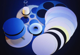
Polishing
Any defects and particles which were created in previous process are removed. In addition, super flat wafers are created by polishing. After the polishing process, wafers are mirrored and without deformation.
- Cleaning
- Inspection
- Packing and shipping
Complete
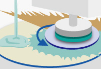
Polishing of NITTA DuPont
In the polishing process, wafer surface is polished with fine particles and polishing pads which are compound with a special felt or plate-shaped pad of several millimeters thickness. NITTA DuPont provides major consumable materials such as polishing pads and slurries and fixturing which are used in the polishing process.