


Silicon wafers are manufactured from ingots through the slicing process, grinding process, polishing process, and cleaning process.
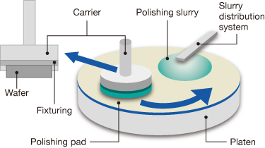
The major purpose of the polishing process is the removal of the defect layer which is generated by the grinding process. Furthermore, on its completion, it requires a high flatness, defect-free, uncontaminated surface as well. The planarized surface of Silicon wafer down to nanometer level enables a shiny mirror-like appearance.
Semiconductor device wafers are semiconductor chips made through sub-micron level wiring implemented atop silicon wafers. The wiring uses multiple layers which lead to unevenness, requiring the surface to be flattened. Polishing is conducted at this point with the removal of uneven points due to wiring playing a major role.

It seems to be simple, but perfect sphere or perfect flatness theoretically can not exist in the Natural World. However, most-advanced Technology and Science pursue this “Perfection” and “Absolute”. This is not a challenge against Nature, but seeking spirit to the mystery of Nature and a challenge to the possibilities given to the Humans.