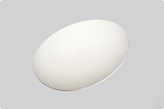
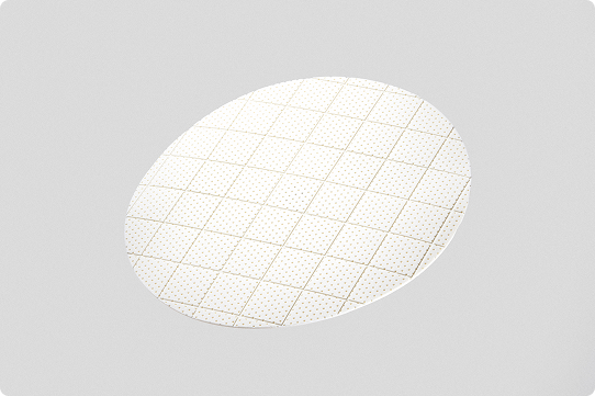
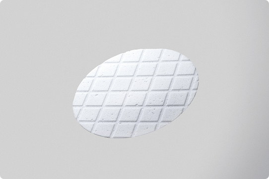
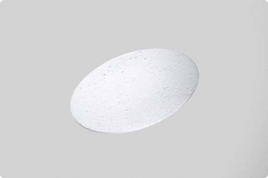
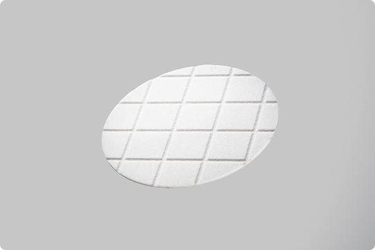
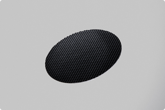
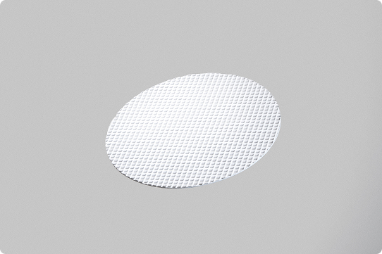
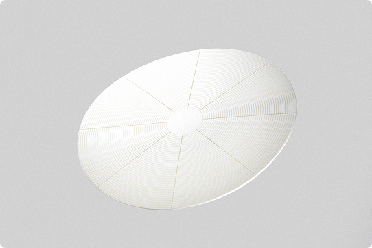
Ikonic™4121H
- Application
- Semiconductor
- Process
- Cu bulk ・ Tungsten ・ STI
- Function
- High removal rate ・ Low erosion ・ Wafer defect reduction
The Ikonic™ Series is a revolutionary CMP pad platform that has multiple uses and supports state-of-the-art nodes. The cutting-edge CMP polishing pad technologies used in this series combines a range of pad hardnesses and varying porosities to create easily adjustable pad surfaces. They are designed to reduce the frequency of wafer defects, improve polishing efficiency and flatness, and improve process costs for customers.
Supreme™, MH™, EXTERION™, ILD™, Nanopure™ and Machplaner™ are trademarks of NITTA DuPont Incorporated.
IC1000™ is a trademark or service mark of NITTA DuPont Incorporated or affiliates of DuPont de Nemours, Inc.
Suba™, VisionPad™, Ikonic™, Optivision™, Acuplane™, Optiplane™ and Novaplane™ are trademarks, service marks or registered trademarks of affiliates of DuPont de Nemours, Inc.
DiaGrid ® and Pyradia ® are registered trademarks of KINIK Company.